Welcome To Cardenas Lab
Cardenas Lab is a fun research group working to transform how people do science and technology using nanoscale optical devices.
We do optics on a chip by engineering structures at the nanoscale level using microfabrication techniques.
We work with any materials needed for our application ranging from recently discovered 2D materials all the way to glass.
Some examples of the questions we want to answer or problems we want to solve are:
- How do you package photonic devices for low cost and high volume applications?
- What tools can be conceived and built that will revolutionize other scientific fields such as neuroscience, cellular biology, or astronomy?
- What new platform will revolutionize nanophotonics?
In our lab you will design and fabricate nanophotonic devices to solve (or answer) some of today’s challenging problems (or questions).

Our Mission
To prepare students for their career goals in industry or academia.
To revolutionize science and technology in interdisciplinary fields using photonics.
To transform the field of photonics using novel materials, techniques, and devices.
Who We Are


Research
Our current research areas are in novel optical materials and devices and packaging


Latest Publications
Ultrabroadband, High Color Purity Multispectral Color Filter Arrays
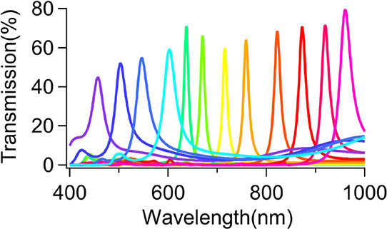
Multispectral imagers that capture spatiospectral information are of growing importance in various fields, particularly in remote sensing and metrology. To enable integrated snapshot multispectral imagers and eliminate the drawbacks of traditional systems, such as bulkiness and slow scanning mechanisms, miniature, broadband multispectral filter arrays with narrow line widths, high transmission, and Complementary Metal Oxide Semiconductor (CMOS) compatibility are essential. However, current miniature transmissive filter arrays, primarily based on diffractive nanostructures, suffer from limitations such as small working bandwidth, low transmission, poor color purity, and sensitivity to polarization and incident angles.Toaddressthesechallenges,wepresentahigh-orderFabry−Peŕot multispectral filter array (MSFA) with selective peak suppression, leveraging subwavelength nanostructures for filter tuning without changing the physical thickness and employing an ultrathin metal layer to exploit high-order resonances, significantly extending the working range and spectral resolution. High color purity across a broad range (400−1000 nm) is made possible through optical absorption from polysilicon and selective suppression from a platinum layer. The fabricated color filter arrays cover wavelengths from 622 to 960 nm, with full width at half-maximum (FWHM) ranging from 13 to 31 nm and average transmissions exceeding 60%. Our filters also show low sensitivity to oblique incident angles of up to 30° with minimal wavelength shifts. Furthermore, these filters can be downscaled to sizes compatible with modern CMOS imagers, reaching dimensions as small as 1 μm. The introduction of a resonance combining design further extends the working range (455−960 nm), aligning with the capabilities of silicon photodetectors. Its adaptability across wavelength ranges and potential for tunable applications hold promise for transformative imaging and display technologies across a wide spectrum.
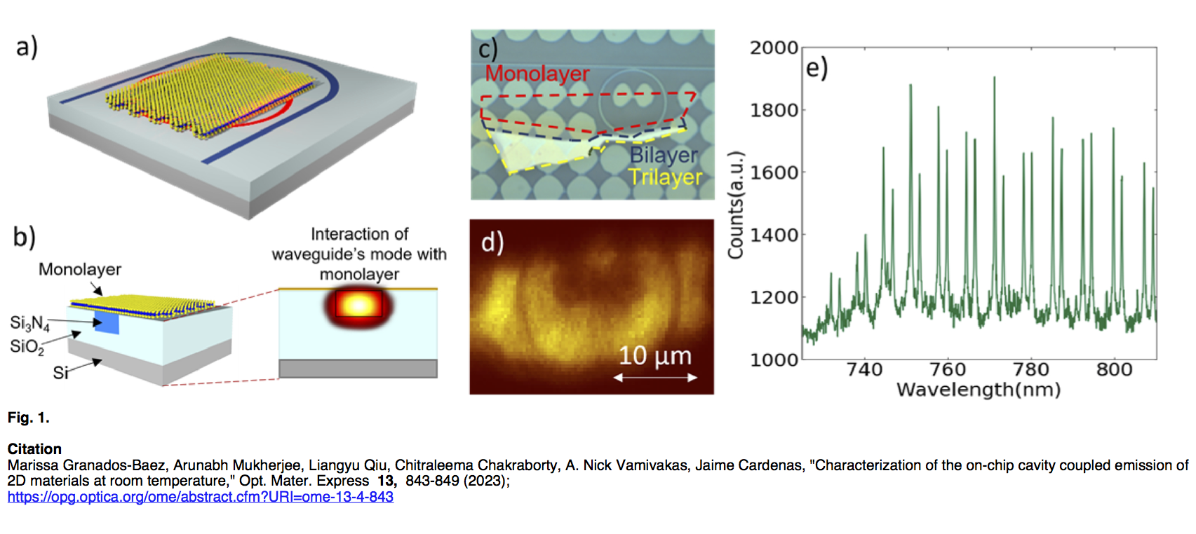
Characterization of the on-chip cavity coupled emission of 2D materials at room temperature
Light sources or lasers based on two-dimensional (2D) materials have been recently demonstrated with different photonic cavities emitting into free space. However, on-chip lasing based on 2D materials remains challenging. We present the characterization of on-chip cavity coupled emission from 2D materials and observe laser-like emission properties. We report 30% linewidth narrowing and a ‘kink’ in the input vs. output power relation of a device consisting of a monolayer WSe2 monolithically integrated with a high-quality factor microring resonator operating at room temperature. Our device could ultimately enable fully integrated devices where all on-chip active functionalities are mediated by 2D materials.
Engineered Second-Order Nonlinearity in Silicon Nitride.
We overcome this drawback and demonstrate a successful induction of χ(2) in Si3N4 through electrical poling with an externally-applied field to align the Si-N bonds. This alignment breaks the centrosymmetry of Si3N4, and enables the bulk χ(2). The sample is heated to over 500°C to facilitate the poling. The comparison between the EO responses of poled and non-poled Si3N4, measured using a Si3N4 micro-ring modulator, shows an enhancement in the amplitude of the measured EO responses as well as a remarkable improvement in its speed from 3GHz to at least 15GHz (3dB bandwidth) after the poling, which confirms the χ(2) nature of the EO response induced by poling.
Adiabatic Frequency Conversion
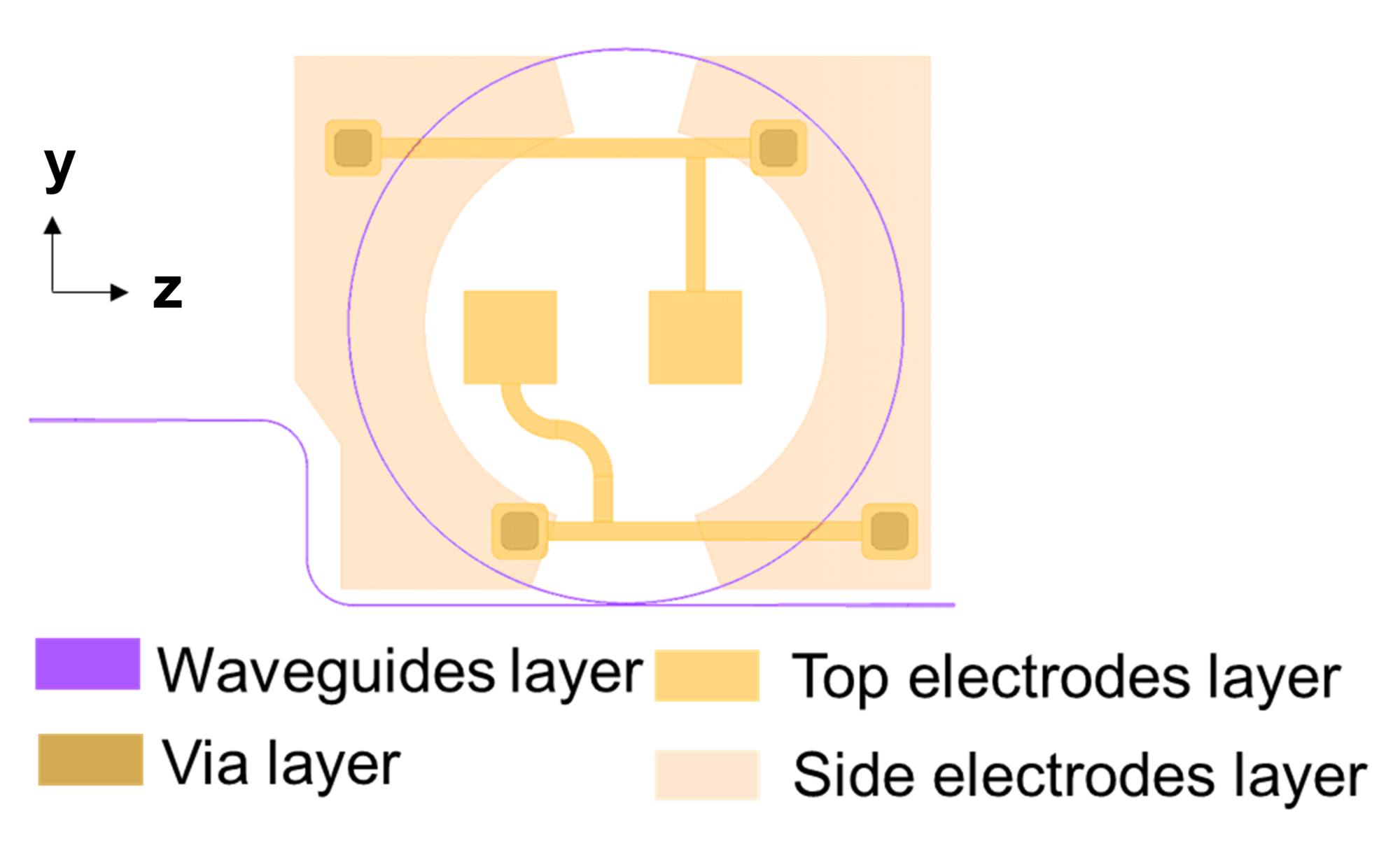
Changing the frequency of light outside the laser cavity is essential for an integrated photonics platform, especially when the optical frequency of the on-chip light source is fixed or challenging to be tuned precisely. To achieve continuous on-chip optical frequency conversion, we apply adiabatic frequency conversion to a lithium niobate ring resonator. To be specific, we fabricate Lithium niobate ring resonator with a pair of electrodes on the side of the waveguide, which can apply electric field to change the refractive index of the waveguide based on Pockels effect, resulting in resonance shift. The light trapped inside the cavity will also shift its frequency together with the resonance. Just like tuning the frequency of sound on a vibrating guitar string by changing the string length! To achieve continuous frequency tunning, we only need to adjust the voltage applied. In this work, frequency shifts of up to 14.3 GHz are achieved by adjusting the voltage of an RF control. With this technique, we can dynamically control light in a cavity within its photon lifetime by tuning the refractive index of the ring resonator electrically, which will have potential application in Frequency Modulated Continuous Wave (FMCW) Lidar.
Our Sponsors


