Research Focus
Cardenas Lab research focuses on integrated photonics, nanophotonics, and nonlinear photonics. Our group tackles high impact challenges using nano-structured devices on a chip. Current research is focused on four main areas:


Photonic Packaging
One of the biggest challenges in the mass manufacturing of photonic chips is the fiber to the chip attachment process. The current method of attaching an optical fiber to a photonic chip uses active alignment and adhesive to secure it in place. Adhesives are susceptible to environmental fluctuations and shrink during the curing process. On average curing of adhesives takes 5-10mins of tool time in a process line, this leads to increased production costs. About 80% of the total cost of a photonic device is from packaging and testing and approximately 80% of that is the fiber-attach process. Optical transceivers are the heart and soul of a data center. Nearly all our data communication over the internet, like, zoom calls, online conferences, uses data centers to process and transmit the data. Therefore, speed, performance, and low operating cost are very vital for the data centers.
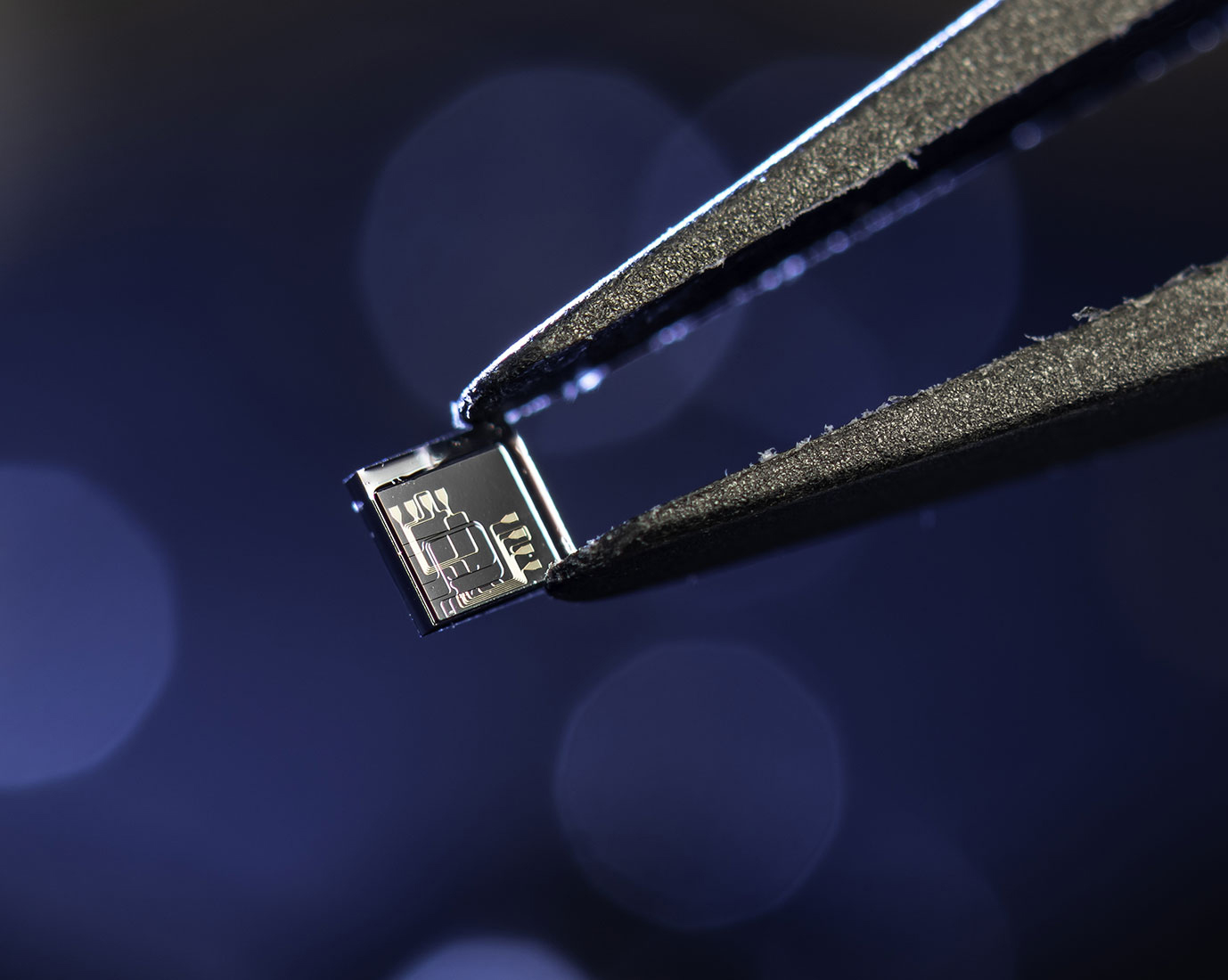
We introduce a novel method for connecting optical fibers to integrated photonic chips using a laser [Nauriyal, Juniyali, et al. Optica 6.5 (2019): 549-552.] To improve the device performance, we introduce an oxide mode converter which helps in matching the mode of an optical fiber to the mode of the photonic chip. This oxide mode converter is a waveguide carved out from the silicon dioxide substrate of the photonic chip with air as its cladding. It also acts as an interface for attaching the photonic chip to the optical fiber. To make this coupling process permanent we use a carbon dioxide laser to melt the optical fiber to the photonic chip. An optical fiber is made up of glass/silicon dioxide and the photonic chip has a thick substrate of glass/silicon dioxide. We use a laser to melt them together to form a fusion bond between the glass-to-glass interface making this technology mechanical more robust.
We demonstrated a 1dB coupling loss per facet between an optical fiber and a photonic chip at 1550nm of laser wavelength. This is to our knowledge the lowest recorded loss in a completely packaged photonic device.
Nauriyal, Juniyali, et al. “Fiber-to-chip fusion splicing for low-loss photonic packaging.” Optica 6.5 (2019): 549-552.
On-Chip Weak Value Amplification
Optical interferometry has been a significant part of sensing and metrology. From gyroscope and surface examination to gravitational wave detection, optical interferometers are widely used for precision measurements. Weak value amplification is a technique that allows interferometric signal enhancement without amplifying technical noises.
We implement weak value amplification on an integrated Mach-Zehnder interferometer by spatial and temporal phase engineering of the optical wave in waveguides. We achieve 7 dB signal-to-noise ratio improvement over standard integrated Mach-Zehnder interferometer (equal detected optical power) in a heat-induced phase shift measurement. Also, by adding ring resonator to the weak value interferometer as dispersive element, we detect an optical frequency shift down to 2 kHz.
Song, Meiting, et al. “Enhanced on-chip phase measurement by inverse weak value amplification.” Nature Communications 12.1 (2021): 1-7.


AI For Manufacturing
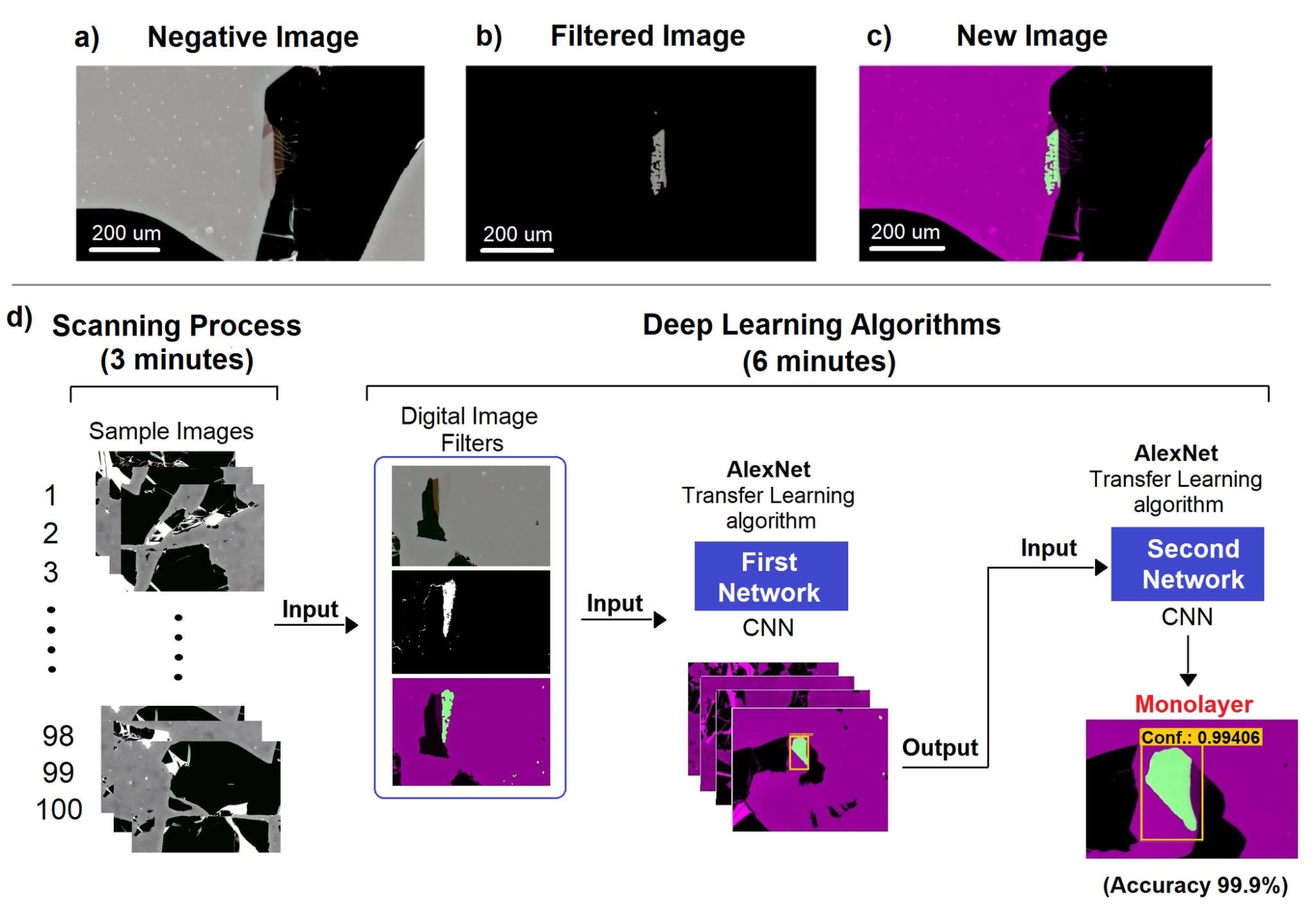
The unique properties of two-dimensional materials for light emission, detection, and modulation make them ideal for integrated photonic devices. However, identifying if the films are indeed monolayers is a time-consuming process even for well-trained operators.
We develop an intelligent algorithm to detect monolayers of WSe2, MoS2 and h-BN autonomously using Digital Image Processing and Deep Learning with high accuracy rate, avoiding human interaction and any additional characterization tests.
J. Sanchez-Juarez, M. Granados-Baez, A. A. Aguilar-Lasserre, and J. Cardenas, “Automated system for the detection of 2D materials using digital image processing and deep learning,” Opt. Mater. Express 12, 1856 (2022).

Engineered Second-Order Nonlinearity in Silicon Nitride
Silicon nitride (Si3N4) is a low-loss, CMOS-compatible material platform widely used in integrated photonics. Si3N4 films deposited in the foundry, usually through low pressure chemical vapor deposition (LPCVD) or plasma enhanced chemical vapor deposition (PECVD), are amorphous (therefore, centrosymmetric). Such symmetry leads to a lack of second-order nonlinearity (χ(2)) in Si3N4 which keeps it from key active functions such as Pockels electro-optic (EO) modulation and efficient second harmonic generation (SHG). We overcome this drawback and demonstrate a successful induction of χ(2) in Si3N4 through electrical poling with an externally-applied field to align the Si-N bonds.
Zhang, Yi, et al. “Engineered second-order nonlinearity in silicon nitride.” Optical Materials Express 13.1 (2023): 237-246.

Adiabatic Frequency Conversion
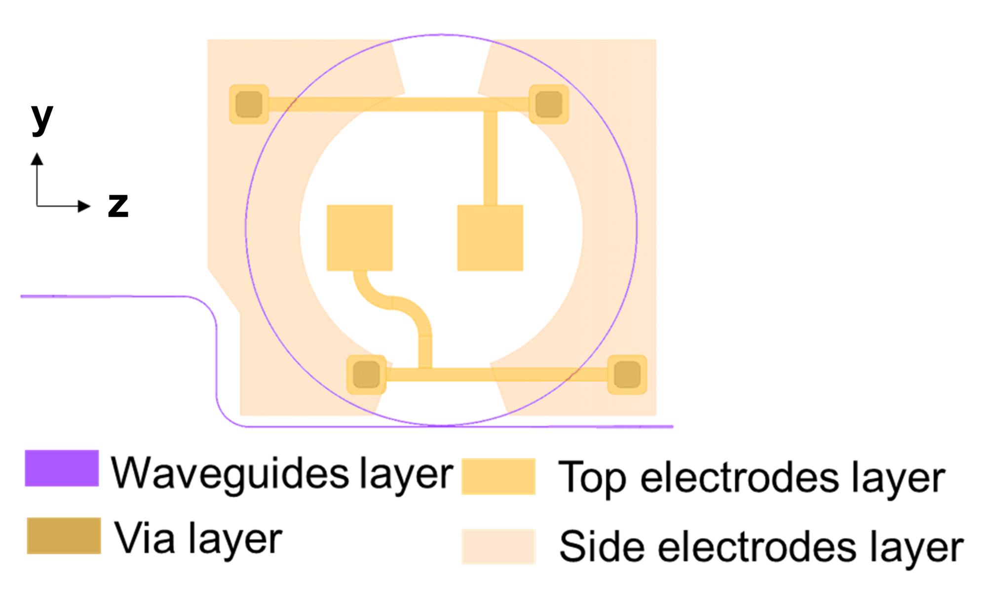
Changing the frequency of light outside the laser cavity is essential for an integrated photonics platform, especially when the optical frequency of the on-chip light source is fixed or challenging to be tuned precisely. To achieve continuous on-chip optical frequency conversion, we apply adiabatic frequency conversion to a lithium niobate ring resonator. To be specific, we fabricate Lithium niobate ring resonator with a pair of electrodes on the side of the waveguide, which can apply electric field to change the refractive index of the waveguide based on Pockels effect, resulting in resonance shift. The light trapped inside the cavity will also shift its frequency together with the resonance. Just like tuning the frequency of sound on a vibrating guitar string by changing the string length! To achieve continuous frequency tunning, we only need to adjust the voltage applied. In this work, frequency shifts of up to 14.3 GHz are achieved by adjusting the voltage of an RF control. With this technique, we can dynamically control light in a cavity within its photon lifetime by tuning the refractive index of the ring resonator electrically, which will have potential application in Frequency Modulated Continuous Wave (FMCW) Lidar.
Our AFC work is a collaboration with the group of Professor Govind Agrawal.
X. He, L. Cortes-Herrera, K. Opong-Mensah, Y. Zhang, G. P. Agrawal, and J. Cardenas, “Electrically induced adiabatic frequency conversion in an integrated lithium niobate ring resonator,” Opt. Letters, 47(22), 5849 – 5852 (2022). 10.1364/OL.473113.
L. Cortes-Herrera, X. He, J. Cardenas, and G.P. Agrawal, “Design of an X-cut thin-film lithium niobate waveguide as a passive polarization rotator,” Opt. Express 29(26), 44174 – 44188 (2021).
L. Cortes-Herrera, X. He, J. Cardenas, and G. P. Agrawal, “Coupled-mode theory of the polarization dynamics inside a microring resonator with a uniaxial core,” Phys. Rev. A 103 (6), 063517 (2021).


